High End Semiconductor Packaging Market Size 2025-2029
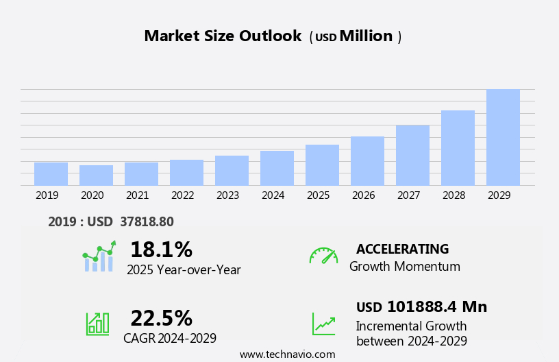
The high end semiconductor packaging market size is forecast to increase by USD 101.89 billion at a CAGR of 22.5% between 2024 and 2029.
- The market is experiencing significant growth, driven primarily by the increasing demand for compact electronic devices and surging investments in 5G technology. The compactness and efficiency of these devices necessitate advanced semiconductor packaging solutions, fueling market expansion. However, the market's growth potential is tempered by challenges, including the high manufacturing cost of high end semiconductor packaging due to warping issues. This problem arises from the use of advanced materials and complex processes, which can lead to dimensional instability during manufacturing. The increasing demand for compact electronic devices, such as smartphones and laptops, is driving the market's expansion. Additionally, the increase in investments towards the implementation of 5G technology is boosting the market's growth.
- Additionally, regulatory hurdles impact adoption, as stringent regulations governing the use of certain materials and manufacturing processes add complexity to the market landscape. To capitalize on market opportunities and navigate these challenges effectively, companies must focus on innovation, cost reduction strategies, and regulatory compliance. By addressing these issues, they can differentiate themselves in the competitive market and secure a strong market position.
What will be the Size of the High End Semiconductor Packaging Market during the forecast period?
- The high-end semiconductor packaging market is driven by industry standards and emerging technologies that cater to high-end applications. The packaging roadmap is shaped by Moore's Law extension and advanced substrate technology, pushing the boundaries of high-density interconnection and performance enhancement. Industry collaboration plays a crucial role in the development of innovative hubs, where packaging line automation, package design software, and packaging process control are prioritized. Electromagnetic interference and high-frequency packaging are key challenges addressed through chip-scale packaging solutions, such as silicon interposers, which enhance power efficiency and reduce thermal dissipation. Next-generation devices require advanced packaging techniques to ensure reliability and address electromagnetic interference and electrostatic discharge issues. The market is experiencing significant growth, driven by the increasing demand for smart devices and consumer IoT devices.
- Failure analysis and packaging simulation tools are essential for optimizing design and mitigating risks in the manufacturing process. Moore's Law continues to influence the market, necessitating the adoption of multi-chip module technology and the integration of industry standards to accommodate the increasing complexity of semiconductor components. The industry is witnessing a shift towards advanced packaging technologies such as microelectronics packaging, packaging automation, and packaging simulation. Furthermore, the packaging process involves the assembly of semiconductor components, such as microchips, integrated circuits, and consumer electronics components, onto silicon wafers. High-end applications, such as artificial intelligence and 5G infrastructure, demand advanced packaging solutions to meet their power and performance requirements. The semiconductor packaging industry remains a dynamic and evolving landscape, with a focus on continuous innovation and improvement.
How is this High End Semiconductor Packaging Industry segmented?
The high end semiconductor packaging industry research report provides comprehensive data (region-wise segment analysis), with forecasts and estimates in "USD million" for the period 2025-2029, as well as historical data from 2019-2023 for the following segments.
- End-user
- Consumer electronics
- Telecom and datacom
- Automotive
- Others
- Technology
- 3D SoC
- 3D stacked memory
- 2.5D interposers
- UHD FO
- Embedded Si bridge
- Material
- Organic substrates
- Bonding wires
- Lead frames
- Encapsulation resins
- Others
- Geography
- North America
- US
- Canada
- Mexico
- Europe
- France
- Germany
- UK
- APAC
- China
- India
- Japan
- South America
- Brazil
- Rest of World (ROW)
- North America
By End-user Insights
The consumer electronics segment is estimated to witness significant growth during the forecast period. In the semiconductor industry, consumer electronics is a significant end-market. The growth of this sector is driven by the expanding smartphone market, increasing adoption of wearable and smart devices, and rising penetration of the Internet of Things (IoT) in applications like smart homes. With the advent of 5G technology, semiconductor manufacturers anticipate widespread adoption of 5G smartphones featuring higher silicon content. These devices require improved power efficiency, faster speeds, and advanced functionalities, leading to an increase in the number of semiconductor components per device. Consequently, the demand for semiconductor packaging solutions, including through-silicon vias (TSVs), flip-chip packaging, wafer-level packaging, and fan-out packaging, is projected to in the consumer electronics sector.
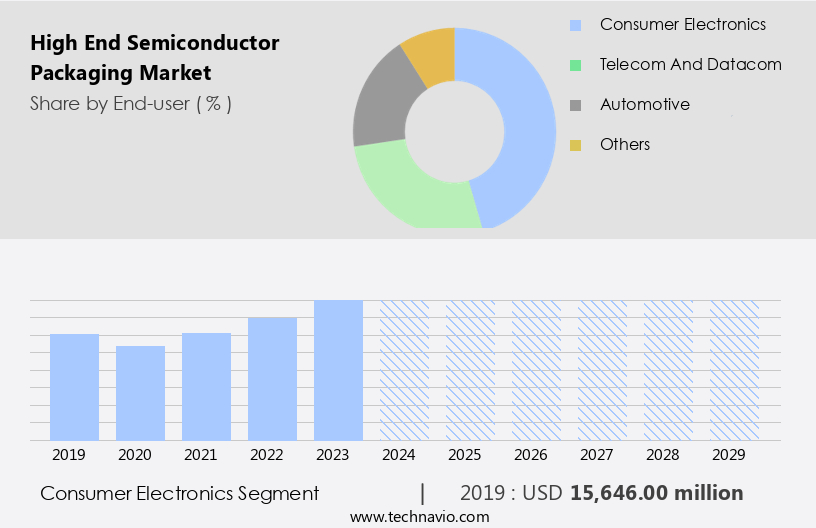
The Consumer electronics segment was valued at USD 15.65 billion in 2019 and showed a gradual increase during the forecast period. Advanced materials, such as dielectric materials and solder alloys, play a crucial role in ensuring reliability and yield optimization. Additionally, packaging technologies like ball grid array (BGA), 2.5D packaging, and 3D packaging, contribute to signal integrity and thermal management. The integration of machine learning, artificial intelligence, and power management systems further enhances the functionality of these devices. The automotive electronics, data center, and industrial sectors also benefit from these advanced packaging solutions, as they require high-performance computing and heterogeneous integration for power efficiency and cost optimization.
Regional Analysis
APAC is estimated to contribute 32% to the growth of the global market during the forecast period. Technavio's analysts have elaborately explained the regional trends and drivers that shape the market during the forecast period.
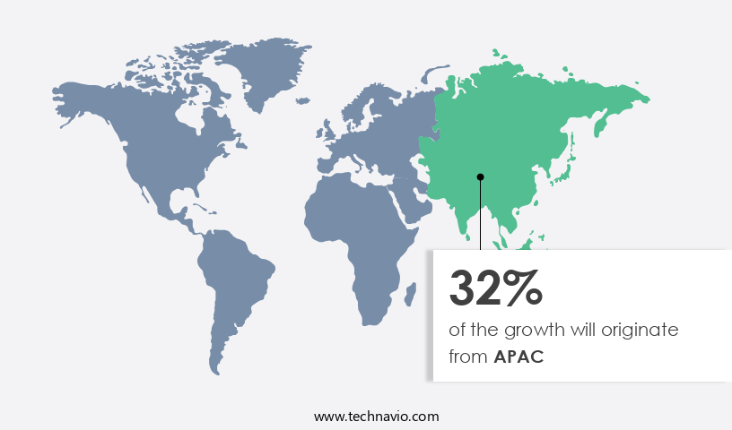
The market is experiencing significant growth in APAC, driven by the presence of major semiconductor foundries, including United Microelectronics, Samsung Electronics, and Semiconductor Manufacturing International. These companies are investing heavily in building new manufacturing facilities to meet the increasing demand for advanced semiconductor technologies. For instance, Semiconductor Manufacturing International recently opened its largest 300mm wafer manufacturing facility in Shanghai. Moreover, the proliferation of mobile devices, data centers, automotive electronics, machine learning, and the Internet of Things (IoT) is fueling the need for high-performance semiconductor devices. Advanced packaging technologies, such as through-silicon vias (TSVs), flip-chip packaging, wafer-level packaging, fan-out packaging, and 2.5D packaging, are essential for these applications due to their ability to improve signal integrity, thermal management, and yield optimization.
Advanced materials, such as dielectric materials and solder alloys, play a crucial role in the development of these packaging technologies. Reliability testing and cost optimization are also critical factors that are driving innovation in the market. Three-dimensional (3D) packaging, heterogeneous integration, and wire bonding are some of the emerging trends in the market. Power management and interconnect technology are essential components of advanced semiconductor devices. Artificial intelligence (AI) and machine learning are also increasingly being integrated into semiconductor devices, leading to the development of new packaging solutions. Overall, the market is expected to continue its growth trajectory, driven by the increasing demand for high-performance semiconductor devices in various industries, including telecommunications, automotive, and consumer electronics.
Market Dynamics
Our researchers analyzed the data with 2024 as the base year, along with the key drivers, trends, and challenges. A holistic analysis of drivers will help companies refine their marketing strategies to gain a competitive advantage.
What are the High End Semiconductor Packaging market drivers leading to the rise in the adoption of Industry?
- The increasing preference for portable electronic devices is the primary market catalyst, driven by advancements in technology that enable smaller, more efficient devices. The semiconductor industry is experiencing significant growth due to the increasing demand for compact electronic devices in various sectors, including communication, automotive, industrial manufacturing, and healthcare. This trend has driven IC manufacturers to invest heavily in research and development to minimize IC size while maximizing performance. The result has been the emergence of micro-electromechanical systems (MEMS) and 3D IC chips. High-end semiconductor packaging plays a crucial role in this evolution by integrating multiple ICs and components into a single package, thereby providing a highly integrated solution with reduced size and enhanced performance. Dielectric materials, a key component of semiconductor packaging, ensure reliable electrical insulation and thermal management.
- Cost optimization and yield optimization are critical considerations in the semiconductor packaging market, with solder balls and other interconnect solutions playing a significant role in achieving these objectives. Thermal management is another essential aspect, as efficient heat dissipation is necessary to maintain the reliability and longevity of semiconductor devices, particularly memory chips. The demand for compact, high-performance electronic devices is driving the adoption of advanced semiconductor packaging technologies. The integration of multiple ICs and components into a single package using dielectric materials, cost-effective interconnect solutions, and efficient thermal management techniques is crucial for achieving the desired size, performance, and reliability.
What are the High End Semiconductor Packaging market trends shaping the Industry?
- The investment landscape is shifting towards an increase in 5G technology, which is emerging as the next major market trend. Companies are allocating significant resources to 5G projects, reflecting this growing trend in the industry. The market is experiencing significant growth due to the increasing demand for advanced electronic components and modules in the next generation communication technology, 5G. With 5G networks set to support data download speeds of up to 10,000 Mbps, there is a pressing need for semiconductor devices that can process and transmit data at much faster rates. High end semiconductor packaging plays a crucial role in achieving these high data rates by reducing signal losses and improving signal integrity. The global investments in 5G infrastructure are expected to accelerate the developments in electronic components and modules, including 5G mm-wave antenna modules, 5G multimode modems, 5G base stations, and various RF products.
- The Internet of Things (IoT), wearable electronics, power management, and RF devices are other sectors that are driving the demand for high end semiconductor packaging. Technologies such as fan-out packaging and 2.5D packaging are gaining popularity due to their ability to accommodate larger and more complex semiconductor designs. Overall, the market is poised for substantial growth in the coming years as the demand for advanced electronic components and modules continues to rise.
How does High End Semiconductor Packaging market faces challenges face during its growth?
- The escalating manufacturing costs of high-end semiconductor packaging, primarily due to warping, pose a significant challenge and hinder the growth of the semiconductor industry. The market faces the challenge of warpage, a distortion that causes the molded part's surface to deviate from the intended design shape. This issue increases manufacturing costs due to wafer wastage. Warpage can occur during various stages of advanced packaging, such as post-mold cure of the reconstituted wafer or back grinding of the epoxy mold compound to expose copper contact pads. Signal integrity is crucial in semiconductor packaging, and warpage can negatively impact it. To mitigate this issue, advanced packaging technologies like artificial intelligence and machine learning are being employed for packaging design and interconnect technology development.
- Heterogeneous integration, wire bonding, and solder alloys are also being used to improve packaging performance and reduce warpage. High-performance computing applications, such as high-frequency trading and graphics, require advanced packaging solutions with minimal warpage for optimal signal integrity and performance.
Exclusive Customer Landscape
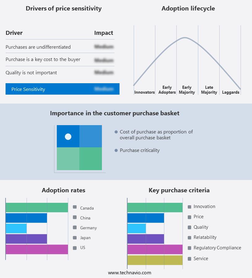
The high end semiconductor packaging market forecasting report includes the adoption lifecycle of the market, covering from the innovator's stage to the laggard's stage. It focuses on adoption rates in different regions based on penetration. Furthermore, the high end semiconductor packaging market report also includes key purchase criteria and drivers of price sensitivity to help companies evaluate and develop their market growth analysis strategies.
Customer Landscape
Key Companies & Market Insights
Companies are implementing various strategies, such as strategic alliances, high end semiconductor packaging market forecast, partnerships, mergers and acquisitions, geographical expansion, and product/service launches, to enhance their presence in the industry.
Advanced Micro Devices Inc. - This company specializes in advanced semiconductor packaging, delivering innovative solutions for high-performance computing (HPC) and artificial intelligence (AI) applications.
The industry research and growth report includes detailed analyses of the competitive landscape of the market and information about key companies, including:
- Advanced Micro Devices Inc.
- Amkor Technology Inc.
- Analog Devices Inc.
- Arm Ltd.
- ASE Technology Holding Co. Ltd.
- Chipbond Technology Corp.
- ChipMOS TECHNOLOGIES Inc.
- Fujitsu Ltd.
- Intel Corp.
- Jiangsu Changdian Technology Co. Ltd.
- King Yuan Electronics Co. Ltd.
- KYOCERA Corp.
- Microchip Technology Inc.
- Nepes Corp.
- Powertech Technology Inc.
- Renesas Electronics Corp.
- Samsung Electronics Co. Ltd.
- Taiwan Semiconductor Manufacturing Co. Ltd.
- Texas Instruments Inc.
- Tongfu Microelectronics Co. Ltd.
Qualitative and quantitative analysis of companies has been conducted to help clients understand the wider business environment as well as the strengths and weaknesses of key industry players. Data is qualitatively analyzed to categorize companies as pure play, category-focused, industry-focused, and diversified; it is quantitatively analyzed to categorize companies as dominant, leading, strong, tentative, and weak.
Recent Development and News in High End Semiconductor Packaging Market
- In February 2024, Intel Corporation announced the launch of its new Foveros 3D packaging technology, which allows for the stacking of multiple chips in a single package to increase performance and reduce power consumption (Intel Press Release, 2024). This development represents a significant technological advancement in the market, as it enables the creation of more complex and powerful semiconductor devices.
- In July 2024, Samsung Electronics and Advanced Semiconductor Engineering Corporation (ASE) formed a strategic partnership to jointly develop and manufacture advanced semiconductor packaging solutions (Samsung Press Release, 2024). This collaboration combines Samsung's semiconductor expertise with ASE's packaging capabilities, aiming to address the growing demand for high-performance, power-efficient semiconductor packaging solutions.
Research Analyst Overview
The market continues to evolve, driven by the relentless pursuit of improved performance, reliability, and cost optimization in various sectors. Through-silicon vias (TSVs) and advanced interconnect technologies, such as ball grid arrays (BGAs), flip-chip packaging, and wafer-level packaging, enable enhanced signal integrity and faster data transfer in applications ranging from high-performance computing and data centers to mobile devices and automotive electronics. Advanced materials, including dielectric materials and solder alloys, play a crucial role in addressing the challenges of thermal management and yield optimization. The integration of machine learning and artificial intelligence in semiconductor packaging design further enhances the industry's ability to optimize processes and improve product performance.
Three-dimensional (3D) packaging, fan-out packaging, and heterogeneous integration are emerging trends, offering increased functionality and miniaturization. Packaging assembly, power management, and reliability testing are essential components of the packaging process, ensuring the successful integration of semiconductor devices into various applications. Interconnect technology continues to advance, with innovations in wire bonding and solder balls driving improved performance and reliability. The Internet of Things (IoT), wearable electronics, RF devices, and memory chips all benefit from the ongoing evolution of semiconductor packaging technologies. In the realm of advanced packaging, high-performance computing applications demand ever-increasing processing power and energy efficiency. The integration of advanced packaging techniques, such as TSVs and 3D packaging, enables the creation of more powerful and compact systems.
The semiconductor packaging industry remains a dynamic and innovative field, with ongoing research and development efforts focused on improving performance, reliability, and cost optimization across various applications. The integration of advanced materials, interconnect technologies, and packaging design techniques continues to drive the industry forward, shaping the future of electronics and technology.
Dive into Technavio's strong research methodology, blending expert interviews, extensive data synthesis, and validated models for unparalleled High End Semiconductor Packaging Market insights. See full methodology.
|
Market Scope |
|
|
Report Coverage |
Details |
|
Page number |
222 |
|
Base year |
2024 |
|
Historic period |
2019-2023 |
|
Forecast period |
2025-2029 |
|
Growth momentum & CAGR |
Accelerate at a CAGR of 22.5% |
|
Market growth 2025-2029 |
USD 101.88 billion |
|
Market structure |
Fragmented |
|
YoY growth 2024-2025(%) |
18.1 |
|
Key countries |
US, China, Germany, Canada, Japan, UK, India, France, Brazil, and Mexico |
|
Competitive landscape |
Leading Companies, Market Positioning of Companies, Competitive Strategies, and Industry Risks |
What are the Key Data Covered in this High End Semiconductor Packaging Market Research and Growth Report?
- CAGR of the High End Semiconductor Packaging industry during the forecast period
- Detailed information on factors that will drive the growth and forecasting between 2025 and 2029
- Precise estimation of the size of the market and its contribution of the industry in focus to the parent market
- Accurate predictions about upcoming growth and trends and changes in consumer behaviour
- Growth of the market across APAC, North America, Europe, South America, and Middle East and Africa
- Thorough analysis of the market's competitive landscape and detailed information about companies
- Comprehensive analysis of factors that will challenge the high end semiconductor packaging market growth of industry companies
We can help! Our analysts can customize this high end semiconductor packaging market research report to meet your requirements.
 RIA -
RIA -